Point contact diodes are formed by pressing a metal needle onto a single crystal of germanium or silicon material and then using the current method. Therefore, its PN junction has a small electrostatic capacity and is suitable for high-frequency circuits. Compared with surface junction type, point contact type is less suitable for high current and rectification. Due to its simple structure, it is inexpensive. Below, Xiaoyi brings you a popular science popularization of electronic components, discussing the characteristics, structure, and classification of diodes. Come and take a look!
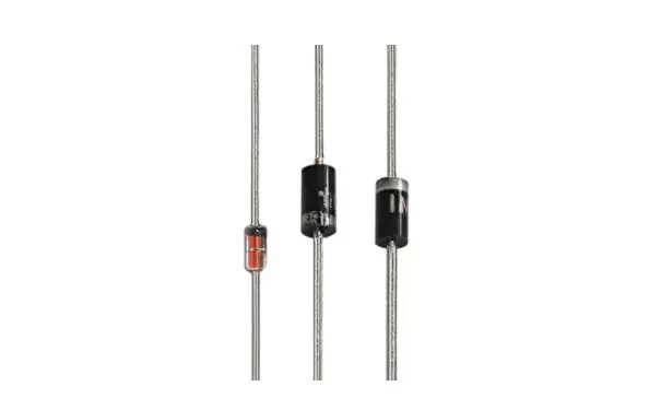
Characteristics of point contact diodes
1. Positive characteristics
In electronic circuits, connecting the positive terminal of a diode to the high potential terminal and the negative terminal to the low potential terminal will cause the diode to conduct. This connection method is called forward bias. It must be noted that when the forward voltage applied across the diode is very small, the diode still cannot conduct, and the forward current flowing through the diode is very weak. Only when the forward voltage reaches a certain value (this value is called the "threshold voltage", also known as the "dead zone voltage", germanium tube is about 0.1V, silicon tube is about 0.5V), can the diode conduct directly and positively. After conduction, the voltage across the diode remains basically unchanged (germanium tube is about 0.3V, silicon tube is about 0.7V), which is called the "forward voltage drop" of the diode.
2. Reverse characteristic
In electronic circuits, the positive terminal of a diode is connected to the low potential terminal, and the negative terminal is connected to the high potential terminal. At this time, there is almost no current flowing through the diode, and the diode is in a cut-off state. This connection method is called reverse bias. When a diode is reverse biased, there will still be a weak reverse current flowing through the diode, which is called leakage current. When the reverse voltage across the diode increases to a certain value, the reverse current will sharply increase, and the diode will lose its unidirectional conductivity characteristics. This state is called diode breakdown.
Structure of point contact diode
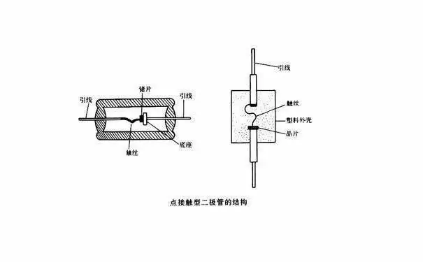
Point contact diodes are made by hot pressing thin metal wires one by one onto a semiconductor wafer. During the hot pressing process, a PN junction is formed on the contact surface between the semiconductor wafer and the metal wire, with the metal wire as the positive electrode and the semiconductor wafer as the negative electrode.
The metal wires of point contact diodes and the metal surfaces of semiconductors are very small, making it difficult to pass large currents. However, due to their small junction capacitance, they can operate at higher frequencies. Point contact diodes can be used in circuits such as detection, frequency conversion, switching, and small current rectification circuits.
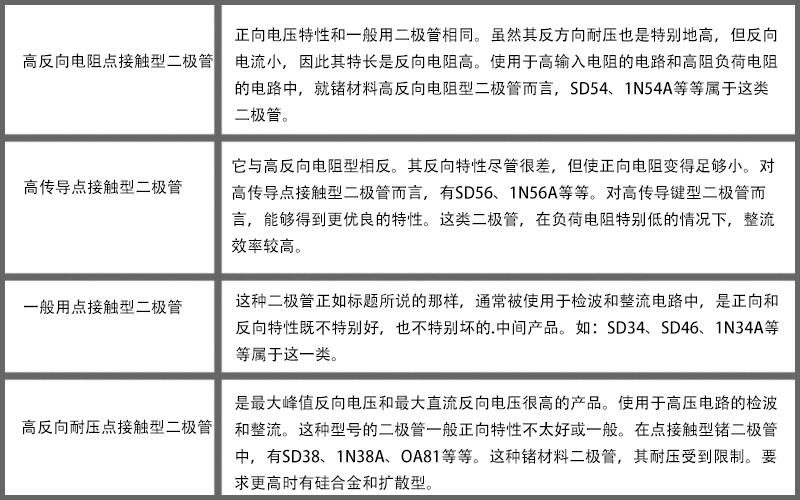
Classification of point contact diodes
